Patent Backed Bankruptcy Report
Company Background:
Lumileds Holding B.V. manufactures and markets light-emitting diodes (LED) and automotive lighting products. It offers COB, color, UV, high power, mid/low power, automotive, display, and flash LEDs; matrix platforms; architectural lighting products, down-lights, high bay and low bay lighting products, indoor area lighting products, lamps, outdoor lighting products, and spotlights. It offers car, truck, and motorcycle lighting products; and LED lighting solutions for televisions, tablets, monitors, cell phones, and public information displays. It serves automotive, consumer, and illumination sectors through distributors worldwide. The company is based in Amsterdam, the Netherlands. Lumileds Holding B.V. operates as a former subsidiary of Koninklijke Philips N.V. On August 29, 2022, Lumileds Holding B.V., along with its affiliates, filed a voluntary petition for reorganization under Chapter 11 in the U.S. Bankruptcy Court for the Southern District of New York.
Address
Ownership
Industry
The Base, Tower B5 Unit 107Evert van de Beekstraat 11118 CL, SchipholThe Netherlands
Private
Semiconductors and Lighting Products
Chapter Type | Case Number | Assets | Liabilities | Industry/Description |
11 | 1:2022bk11161 | $50 Mil – $100 Mil | $100 Mil – $500 Mil | LEDs and Lighting Products |
Portfolio Valuation Range | Asset Valuation Range | Total Assets Valuation Range | Liability Range | Leverage Ratio Range |
$20 Mil – $80.6 Mil | $25 Mil – $100 Mil | $45 Mil – $180.6 Mil | $50 Mil – $375 Mil | 0.1204 – 3.612 |
Patent Portfolio Breakdown
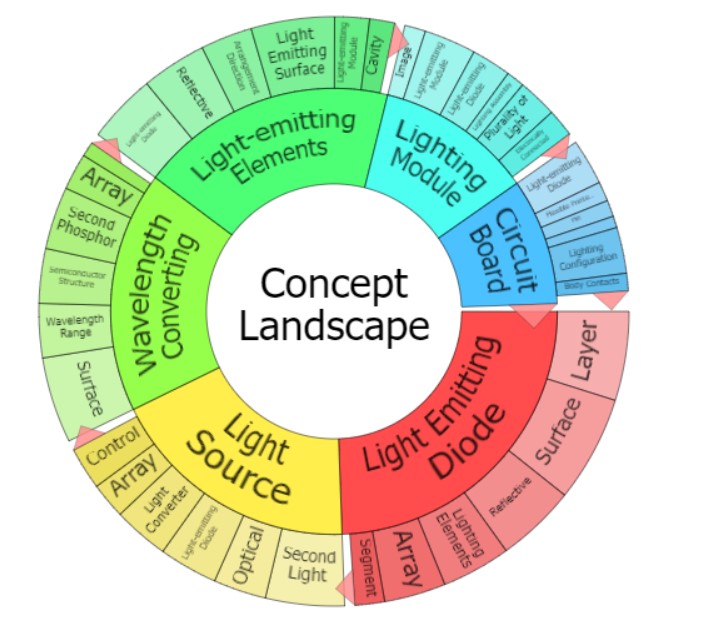
806 Active US Patents

Featured Assets
Abstract:
An optical coupling structure is disposed on a light output surface of a semiconductor LED to facilitate coupling of light emitted by the semiconductor LED through the light output surface. The optical coupling structures comprise light scattering particles and/or air voids embedded in or coated with a thin layer of a material that has an index of refraction close to or matching the index of refraction of the material forming the light output surface of the semiconductor LED.
Claim 1:
A light emitting device comprising:
a semiconductor light emitting diode having a light output surface;
an optical coupling structure disposed on the light output surface, the optical
coupling structure comprising a plurality of light scattering particles coated
with or embedded in a layer of transparent material; and
a wavelength converting structure having a composition that differs from the
optical coupling structure, the optical coupling structure being disposed
between the light output surface and the wavelength converting structure and
being in physical contact with the wavelength converting structure, the layer
of transparent material being in physical contact with the light output surface
and having an index of refraction matching or approximately matching an index
of refraction of the light output surface.
Abstract:
Light emitting diodes (LEDs) having a sensor segment for operational feedback are described. A semiconductor stack is grown on a sapphire substrate. The semiconductor stack is segmented to form at least two segments, where one segment senses light emissions (photosensor segment) from the other segment (emitter segment). The segmentation is achieved by etching a trench or forming a segmentation layer between the segments. One segment can alternate on a predetermined basis between functioning as a photosensor segment or as an emitter segment. The photosensor segment can detect either a side light ray emitting from the emitter segment or a reflected light ray from a substrate. The photosensor segment generates a current based on the detected light ray. A detector circuit can provide operational feedback based on the sensed current.
Claim 1:
A light emitting device, comprising:
a detector circuit; and
a light emitting diode (LED) die including:
a semiconductor stack grown on a substrate, the semiconductor stack including a
n-type layer, an active layer and a p-type layer;
an emitter segment formed from one segment of the semiconductor stack, the emitter
segment configured to emit a light ray;
a photosensor segment formed from another segment of the semiconductor stack, the
photosensor segment configured to sense a reflected light ray from the
substrate and generate a current responsive to the reflected light ray;
a segmentation layer formed between the emitter segment and the photosensor
segment, the segmentation layer electrically isolating the emitter segment from
the photosensor segment;
first electrodes configured to provide power to energize the emitter segment; and
second electrodes configured to send the current to the detector circuit, the detector
circuit configured to convert the current to a signal which provides
operational feedback with respect to the emitter segment.
Abstract:
The invention describes a passive matrix single-color LED display assembly comprising a matrix of row conductor lines and column conductor lines; an array
of direct-emitting LED packages, wherein the anode of each LED package is electrically connected to one of the row conductor lines and the cathode of
that LED package is connected to one of the column conductor lines; and a driver configured to apply a bias voltage to a row conductor line and to apply
a bias voltage to a column conductor line according to an image to be displayed.
Claim 1:
A passive matrix single-colour light emitting diode (LED) display assembly comprising:
a matrix of row conductor lines and column conductor lines, the column conductor lines
including a spring element arranged between neighboring intersections of the
row conductor lines and the column conductor lines;
a layer of electrically insulating material applied onto a surface of the row conductor
line to electrically isolate that row conductor line from any intersecting
column conductor lines;
an array of direct-emitting LED packages, each of the direct-emitting LED packages in
the array comprising an LED mounted on an interposer with an anode electrically
coupled to one of the row conductor lines and a cathode electrically coupled to
one of the column conductor lines enabling individual control of LEDs in the
array; and
a driver configured to apply a row bias voltage to a row conductor line and to apply a
column bias voltage to a column conductor line according to an image to be
displayed.
.


