[vc_row][vc_column][vc_column_text]Suniva Inc. designs and manufactures monocrystalline photovoltaic solar cells and modules for residential, commercial, government, and micro-utility applications. It offers its products through distributors, resellers, and sales representatives in the United States and internationally. Suniva Inc. was formerly known as Solarity Inc. and changed its name to Suniva Inc. in September 2007. The company was founded in 2006 and is headquartered in Norcross, Georgia. As of October 15, 2015, Suniva Inc. operates as a subsidiary of Shunfeng International Clean Energy Limited.[/vc_column_text][/vc_column][/vc_row][vc_row][vc_column][vc_empty_space][vc_tta_tabs][vc_tta_section title=”Company Info” tab_id=”1485966886423-b3803678-c7ec5ac5-4518fd03-b29a”][vc_column_text]
| Address
5765 Peachtree Industrial Blvd Nw www.suniva.com Phone+1 404 477 2700
|
Ownership
Private Industry Solar Energy
|
[/vc_column_text][/vc_tta_section][vc_tta_section title=”Patent-Backed Value Estimation ” tab_id=”1485966886486-c8105d58-76bb5ac5-4518fd03-b29a”][vc_column_text]Suniva Debt-Asset Leverage Estimate
| Chapter Type | Case Number | Assets | Liabilities | Industry/Description |
| 11 | 17-10837 | $10-50 Million | $100 – 500 Million | Solar Energy |
| Portfolio Valuation Range | Asset Valuation Range | Total Assets Valuation Range | Liability Range | Leverage Ratio Range |
| $750,000.00 – $3,750,000.00 | $5,000,000.00 – $50,000,000.00 | $5,750,000.00 – $53,750,000.00 | $10,000,000.00 – $125,000,000.00 | 0.046 – 5.375 |
Patent Portfolio
36 Total Assets
|
 |
[/vc_column_text][/vc_tta_section][vc_tta_section title=”Featured Assets” tab_id=”1485967825251-b275f45c-d8b55ac5-4518fd03-b29a”][vc_column_text]Suniva Portfolio Summary
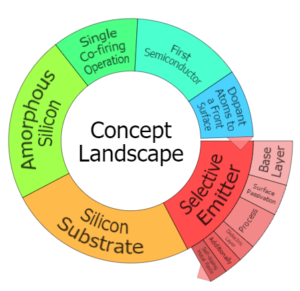
1. US8071418 B2
Title: Selective emitter solar cells formed by a hybrid diffusion and ion implantation process
Abstract: Solar cells and methods for their manufacture are disclosed. An example method may include providing a silicon substrate and introducing dopant to one or more selective regions of the front surface of the substrate by ion implantation. The substrate may be subjected to a single high-temperature anneal cycle. Additional dopant atoms may be introduced for diffusion into the front surface of the substrate during the single anneal cycle. A selective emitter may be formed on the front surface of the substrate such that the one or more selective regions of the selective emitter layer are more heavily doped than the remainder of the selective emitter layer. Associated solar cells are also provided.
First Claim:
A method for forming a selective emitter solar cell by the use of a hybrid diffusion and ion implantation process, comprising:
providing a substrate comprising a base layer;
introducing dopant to one or more selective regions of the front surface of the base layer by ion implantation; and
annealing the substrate, wherein annealing comprises heating the substrate in a furnace to a temperature to:
diffuse additional dopant into the front surface of the base layer, wherein the additional dopant is introduced to the furnace during the anneal; and
form a selective emitter layer on the front surface of the base layer, wherein the one or more selective regions of the front surface of the base layer define one or more selective regions of the selective emitter layer that are more heavily doped than the remainder of the selective emitter layer.
2. US9153728 B2
Title: Ion implanted solar cells with in situ surface passivation
Abstract: Solar cells and methods for their manufacture are disclosed. An example method may include providing a substrate comprising a base layer and introducing n-type dopant to the front surface of the base layer by ion implantation. The substrate may be annealed by heating the substrate to a temperature to anneal the implant damage and activate the introduced dopant, thereby forming an n-type doped layer into the front surface of the base layer. Oxygen may be introduced during the annealing step to form a passivating oxide layer on the n-type doped layer. Back contacts may be screen-printed on the back surface of the base layer, and a p-type doped layer may be formed at the interface of the back surface of the base layer and the back contacts during firing of the back contacts. The back contacts may provide an electrical connection to the p-type doped layer.
First Claim:
A method for manufacturing a solar cell comprising:
providing a substrate comprising a base layer;
introducing dopant to the front surface of the base layer by ion implantation, wherein the dopant introduced is of n-type conductivity;
annealing the substrate, wherein annealing comprises heating the substrate in a furnace to a temperature to:
anneal the implant damage; and
activate the introduced dopant, thereby forming an n-type doped layer into the front surface of the base layer;
introducing oxygen into the furnace during the annealing step to:
form a passivating oxide layer on at least the front surface of the n-type doped layer;
screen-printing one or more back contacts on the back surface of the base layer;
forming a p-type doped layer at the interface of the back surface of the base layer and the one or more back contacts during firing of the one or more back contacts, wherein the one or more back contacts provide an electrical connection to the p-type doped layer.
[/vc_column_text][/vc_tta_section][/vc_tta_tabs][/vc_column][/vc_row][vc_row][vc_column][vc_cta h2=”Portfolio Valuation ” h4=”IPVal offers portfolio valuation services.” add_button=”right” btn_title=”Contact Us ” btn_add_icon=”true” btn_link=”url:http%3A%2F%2Fipval.com%2Fcontact-us%2F%231467647561464-2a34809f-529c||”][/vc_cta][/vc_column][/vc_row][vc_row][vc_column][/vc_column][/vc_row]